- 您现在的位置:买卖IC网 > Sheet目录3818 > PIC18F4620-I/ML (Microchip Technology)IC MCU FLASH 32KX16 44QFN
PIC17C4X
DS30412C-page 54
1996 Microchip Technology Inc.
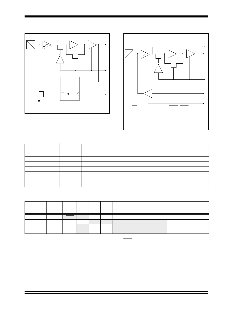
FIGURE 9-2:
RA2 AND RA3 BLOCK
DIAGRAM
Note: I/O pins have protection diodes to VSS.
Data Bus
WR_PORTA
(Q4)
QD
Q
CK
RD_PORTA
(Q2)
FIGURE 9-3:
RA4 AND RA5 BLOCK
DIAGRAM
Note: I/O pins have protection diodes to VDD and VSS.
Data Bus
RD_PORTA
(Q2)
Serial port output signals
Serial port input signal
OE = SPEN,SYNC,TXEN, CREN, SREN for RA4
OE = SPEN (SYNC+SYNC,CSRC) for RA5
TABLE 9-1:
PORTA FUNCTIONS
TABLE 9-2:
REGISTERS/BITS ASSOCIATED WITH PORTA
Name
Bit0
Buffer Type
Function
RA0/INT
bit0
ST
Input or external interrupt input.
RA1/T0CKI
bit1
ST
Input or clock input to the TMR0 timer/counter, and/or an external interrupt input.
RA2
bit2
ST
Input/Output. Output is open drain type.
RA3
bit3
ST
Input/Output. Output is open drain type.
RA4/RX/DT
bit4
ST
Input or USART Asynchronous Receive or USART Synchronous Data.
RA5/TX/CK
bit5
ST
Input or USART Asynchronous Transmit or USART Synchronous Clock.
RBPU
bit7
—
Control bit for PORTB weak pull-ups.
Legend: ST = Schmitt Trigger input.
Address
Name
Bit 7
Bit 6
Bit 5
Bit 4
Bit 3
Bit 2
Bit 1
Bit 0
Value on
Power-on
Reset
Value on all
other resets
(Note1)
10h, Bank 0
PORTA
RBPU
—
RA5
RA4
RA3
RA2
RA1/T0CKI
RA0/INT
0-xx xxxx
0-uu uuuu
05h, Unbanked
T0STA
INTEDG
T0SE
T0CS
PS3
PS2
PS1
PS0
—
0000 000-
13h, Bank 0
RCSTA
SPEN
RC9
SREN
CREN
—
FERR
OERR
RC9D
0000 -00x
0000 -00u
15h, Bank 0
TXSTA
CSRC
TX9
TXEN
SYNC
—
TRMT
TX9D
0000 --1x
0000 --1u
Legend: x = unknown, u = unchanged, - = unimplemented reads as '0'. Shaded cells are not used by PORTA.
Note 1:
Other (non power-up) resets include: external reset through MCLR and the Watchdog Timer Reset.
发布紧急采购,3分钟左右您将得到回复。
相关PDF资料
PIC24HJ256GP210-I/PT
IC PIC MCU FLASH 128KX16 100TQFP
PIC24HJ128GP310A-I/PF
IC PIC MCU FLASH 128KB 100-TQFP
DSPIC33FJ128GP310-I/PF
IC DSPIC MCU/DSP 128K 100TQFP
PIC16C66-20I/SO
IC MCU OTP 8KX14 PWM 28SOIC
DSPIC33FJ128MC510-I/PT
IC DSPIC MCU/DSP 128K 100TQFP
PIC16C66-20I/SP
IC MCU OTP 8KX14 PWM 28DIP
PIC18LF2620-I/SP
IC MCU FLASH 32KX16 28SDIP
PIC16F877-04I/P
IC MCU FLASH 8KX14 EE 40DIP
相关代理商/技术参数
PIC18F4620-I/P
功能描述:8位微控制器 -MCU 64KB 3968 RAM 36 I/O RoHS:否 制造商:Silicon Labs 核心:8051 处理器系列:C8051F39x 数据总线宽度:8 bit 最大时钟频率:50 MHz 程序存储器大小:16 KB 数据 RAM 大小:1 KB 片上 ADC:Yes 工作电源电压:1.8 V to 3.6 V 工作温度范围:- 40 C to + 105 C 封装 / 箱体:QFN-20 安装风格:SMD/SMT
PIC18F4620-I/P
制造商:Microchip Technology Inc 功能描述:IC 8BIT FLASH MCU 18F4620 DIP40
PIC18F4620-I/PT
功能描述:8位微控制器 -MCU 64KB 3968 RAM 36 I/O RoHS:否 制造商:Silicon Labs 核心:8051 处理器系列:C8051F39x 数据总线宽度:8 bit 最大时钟频率:50 MHz 程序存储器大小:16 KB 数据 RAM 大小:1 KB 片上 ADC:Yes 工作电源电压:1.8 V to 3.6 V 工作温度范围:- 40 C to + 105 C 封装 / 箱体:QFN-20 安装风格:SMD/SMT
PIC18F4620-I/PT
制造商:Microchip Technology Inc 功能描述:IC 8BIT FLASH MCU 18F4620 TQFP44
PIC18F4620T-I/ML
功能描述:8位微控制器 -MCU 64KB 3968 RAM 36 I/O RoHS:否 制造商:Silicon Labs 核心:8051 处理器系列:C8051F39x 数据总线宽度:8 bit 最大时钟频率:50 MHz 程序存储器大小:16 KB 数据 RAM 大小:1 KB 片上 ADC:Yes 工作电源电压:1.8 V to 3.6 V 工作温度范围:- 40 C to + 105 C 封装 / 箱体:QFN-20 安装风格:SMD/SMT
PIC18F4620T-I/PT
功能描述:8位微控制器 -MCU 64KB 3968 RAM 36 I/O RoHS:否 制造商:Silicon Labs 核心:8051 处理器系列:C8051F39x 数据总线宽度:8 bit 最大时钟频率:50 MHz 程序存储器大小:16 KB 数据 RAM 大小:1 KB 片上 ADC:Yes 工作电源电压:1.8 V to 3.6 V 工作温度范围:- 40 C to + 105 C 封装 / 箱体:QFN-20 安装风格:SMD/SMT
PIC18F4680-E/ML
功能描述:8位微控制器 -MCU 64KB 3328 RAM w/ECAN RoHS:否 制造商:Silicon Labs 核心:8051 处理器系列:C8051F39x 数据总线宽度:8 bit 最大时钟频率:50 MHz 程序存储器大小:16 KB 数据 RAM 大小:1 KB 片上 ADC:Yes 工作电源电压:1.8 V to 3.6 V 工作温度范围:- 40 C to + 105 C 封装 / 箱体:QFN-20 安装风格:SMD/SMT
PIC18F4680-E/P
功能描述:8位微控制器 -MCU 64KB 3328 RAM w/ECAN RoHS:否 制造商:Silicon Labs 核心:8051 处理器系列:C8051F39x 数据总线宽度:8 bit 最大时钟频率:50 MHz 程序存储器大小:16 KB 数据 RAM 大小:1 KB 片上 ADC:Yes 工作电源电压:1.8 V to 3.6 V 工作温度范围:- 40 C to + 105 C 封装 / 箱体:QFN-20 安装风格:SMD/SMT